(China (Mainland))


Product Summary
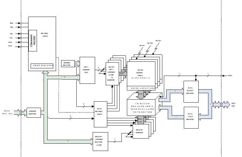
The MT48LC64M4A2P-7E:D is a high-speed CMOS, dynamic random-access memory containing 268,435,456 bits. It is internally configured as a quadbank DRAM with a synchronous interface (all signals are registered on the positive edge of the clock signal, CLK). Each of the x4’s 67,108,864-bit banks is organized as 8,192 rows by 2,048 columns by 4 bits. Each of the x8’s 67,108,864-bit banks is organized as 8,192 rows by 1,024 columns by 8 bits. Each of the x16’s 67,108,864-bit banks is organized as 8,192 rows by 512 columns by 16 bits. Read and write accesses to the MT48LC64M4A2P-7E:D are burst oriented; accesses start at a selected location and continue for a programmed number of locations in a programmed sequence. Accesses begin with the registration of an ACTIVE command, which is then followed by a READ or WRITE command. The address bits registered coincident with the ACTIVE command are used to select the bank and row to be accessed (BA0, BA1 select the bank; A0–A12 select the row). The address bits registered coincident with the READ or WRITE command are used to select the starting column location for the burst access. The MT48LC64M4A2P-7E:D provides for programmable READ or WRITE burst lengths of 1, 2, 4, or 8 locations, or the full page, with a burst terminate option. An auto precharge function may be enabled to provide a self-timed row precharge that is initiated at the end of the burst sequence.
Parametrics
MT48LC64M4A2P-7E:D absolute maximum ratings: (1)Voltage on VDD, VDDQ Supply Relative to VSS: -1V to +4.6V; (2)Voltage on Inputs, NC or I/O Pins Relative to VSS: -1V to 4.6V; (3)Operating Temperature-commercial: 0℃ to +70℃; (4)Operating Temperature-industrial "IT": -40℃ to +85℃; (5)Storage Temperature (plastic): -55℃ to +150℃; (6)Power Dissipation: 1W.
Features
MT48LC64M4A2P-7E:D features: (1)PC66-, PC100-, and PC133-compliant; (2)Fully synchronous; all signals registered on; (3)positive edge of system clock; (4)Internal pipelined operation, column address can be changed every clock cycle; (5)Internal banks for hiding row access/precharge; (6)Programmable burst lengths: 1, 2, 4, 8, or full page; (7)Auto Precharge, includes CONCURRENT AUTO; (8)PRECHARGE, and Auto Refresh Modes; (9)Self Refresh Mode; (10)64ms, 8,192-cycle refresh; (11)LVTTL-compatible inputs and outputs; (12)Single +3.3V ±0.3V power supply.
Diagrams
| Image | Part No | Mfg | Description |  |
Pricing (USD) |
Quantity | ||||||
|---|---|---|---|---|---|---|---|---|---|---|---|---|
 |
 MT48LC64M4A2P-7E:D |
|
IC SDRAM 256MBIT 133MHZ 54TSOP |
Data Sheet |
|
|
||||||
|
MT48LC64M4A2P-7E:D TR |
|
IC SDRAM 256MBIT 133MHZ 54TSOP |
Data Sheet |
|
|
||||||